

Events
HOMEEvents
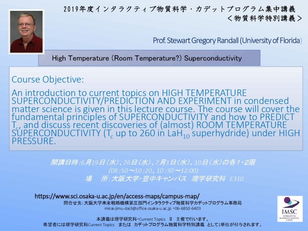
Topical Seminar by Prof. Stewart Gregory Randall
June 19,26, July 3,10
Topical Seminar for IMSC 2019 will be held.
Instructor: Prof. Stewart Gregory Randall (University of Florida)
Title:「High Temperature (Room Temperature?) Superconductivity」
Course Objective:
An introduction to current topics on HIGH TEMPERATURE SUPERCONDUCTIVITY/PREDICTION AND EXPERIMENT in condensed matter science is given in this lecture course. The course will cover the fundamental principles of SUPERCONDUCTIVITY and how to PREDICT Tc, and discuss recent discoveries of (almost) ROOM TEMPERATURE SUPERCONDUCTIVITY (Tc up to 260 in LaH10 superhydride) under HIGH PRESSURE.
Schedule:
June 19 8:50-10:20 10:30-12:00
June 26 8:50-10:20 10:30-12:00
July 3 8:50-10:20 10:30-12:00
July 10 8:50-10:20 10:30-12:00
Place: E310 ,Graduate School of Science ,Toyonaka campus
FY 2019 2nd Solid-State Physics Seminar
2019.6.6(Thu)
FY 2019 2nd Solid-State Physics Seminar
Date:June.6(Thu.) 14:40-16:10
Place:G215, Graduate School of Engineering Science
Lecturer:Distinguished Scientist Koji Azuma(NTT Basic Research Laboratories)
Contact Information:Takashi Yamamoto(D407, Graduate School of Engineering Science)
Tel: 06-6850-6445
E-mail: yamamoto@mp.es.osaka-u.ac.jp
FY 2019 1st Solid-State Physics Seminar
2019.5.23(Thu)
FY 2019 1st Solid-State Physics Seminar
Date:May.23(Thu.) 14:40-16:10
Place:G215, Graduate School of Engineering Science
Lecturer:Director Tetsuya Ido(The Space-Time Standards laboratory, National Institute of Information and Communications Technology)
Contact Information:Takashi Yamamoto(D407, Graduate School of Engineering Science)
Tel: 06-6850-6445
E-mail: yamamoto@mp.es.osaka-u.ac.jp
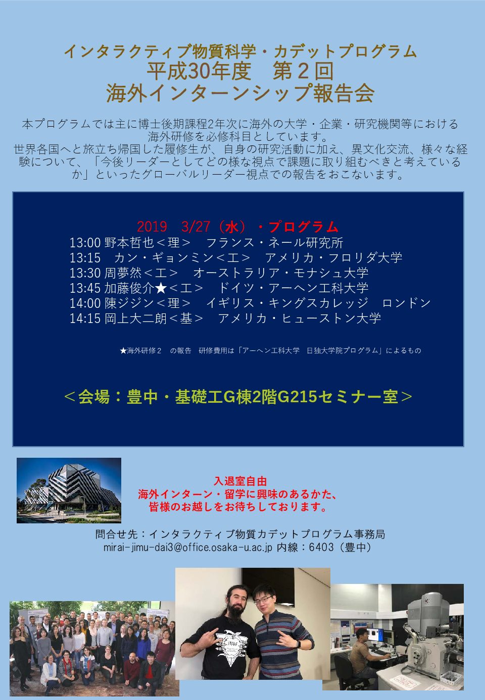
2nd Internship Program (international) Debriefing Session will be held
2019.3.27(Wed)
On March 27, 2nd Internship Program (international) Debriefing Session will be held.
You can join us without reservation.
Date : March 27, 2019 13:00~
Place : G215 (2F of Bulid. G, Graduate School of Engineering Science)
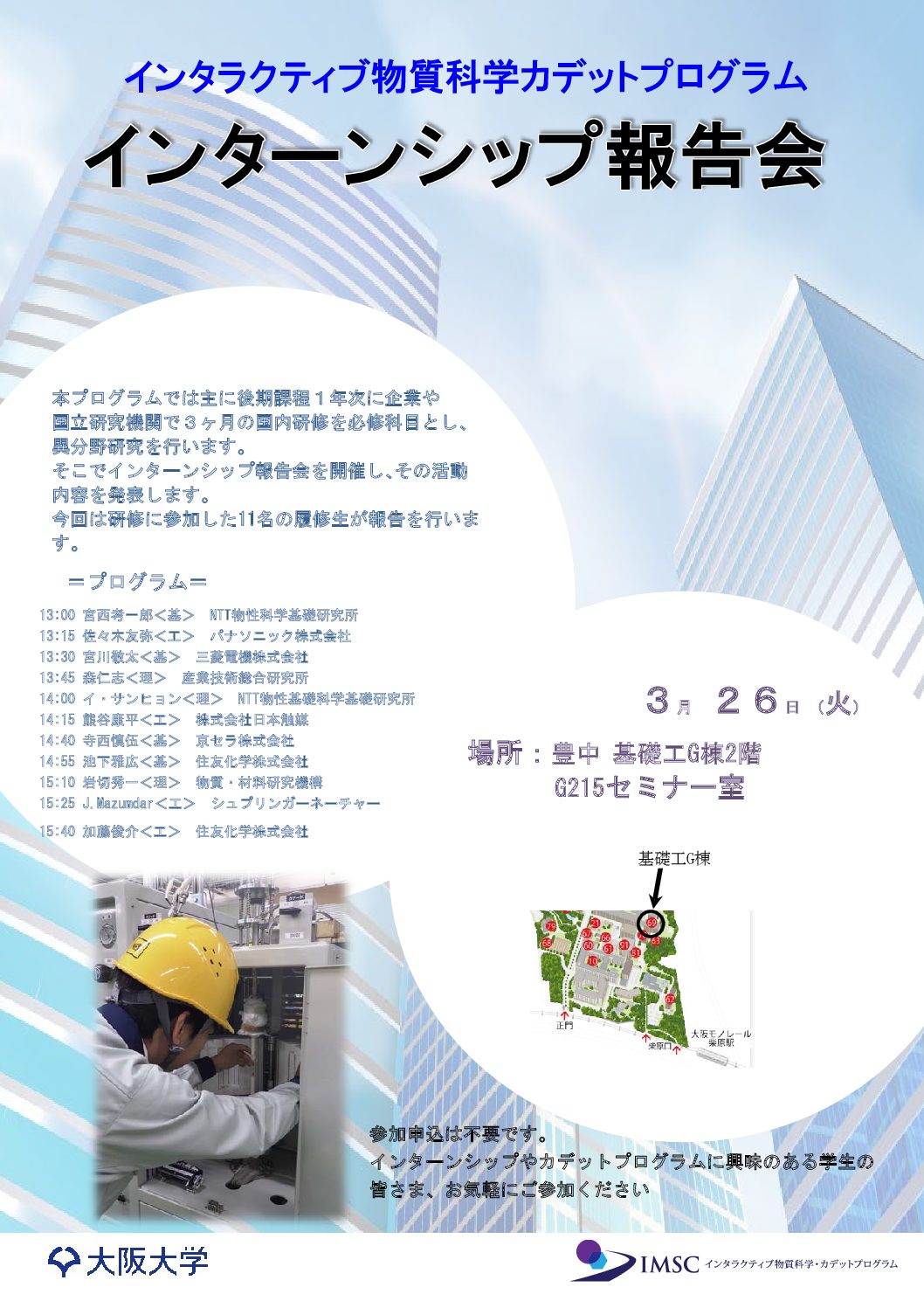
Internship Program (domestic) Debriefing Session will be held
2019.3.26(Tue)
On March 26, Internship Program (domestic) Debriefing Session will be held.
You can join us without reservation.
Date : March 26, 2019 13:00~
Place : G215 (2F of Bulid. G, Graduate School of Engineering Science)
Warning: Trying to access array offset on false in /home/autre/osaka-u.ac.jp/public_html/www.msc/wp-content/themes/imsc/category.php on line 234
Topical Seminar by Prf. Watson Loh of UNICAMP
2019.1.23(Wed)
Topical Seminar for IMSC 2018 will be held.
Lecturer:
Prof. Watson Loh, Institute of Chemistry, UNICAMP, Brazil
(Specially appointed professor of Research Center for Structural Thermodynamics, Osaka University)
Title:
Calorimetry ―Introduction and its application for solutions and other condensed systems―
Purpose:
In this lecture course, thermodynamic properties based on calorimetry of materials and experimental methods of calorimetry are explained. Students who are interested in physical chemistry of materials, solutions, polymers, surfactants, and biological systems can learn from basic points of thermodynamics and how they can apply that idea for materials.
Outline of the course:
In the beginning, fundamental picture of chemical thermodynamics is explained. Then principles of experimental methods and several techniques and apparatuses for calorimetry is given. After understanding the scanning calorimetry and its application in chemistry and biology, the modern technique such as isothermal titration calorimetry (ITC) are explained in detail. The application for kinetics analysis performed by isothermal calorimetry is also studied.
Schedule:
Jan. 23 (Wed.) 1st and 2nd Periods
Jan. 30 (Wed.) 1st, 2nd and 3rd Periods
Feb. 6 (Wed.) 1st, 2nd and 3rd Periods
Place: Graduate School of Science ,Toyonaka campus
Warning: Trying to access array offset on false in /home/autre/osaka-u.ac.jp/public_html/www.msc/wp-content/themes/imsc/category.php on line 234
Topical Seminar by Prf. Ferdi Aryasetiawan of Lund University
2019.1.4(Fri)
Topical Seminar for IMSC 2018 will be held.
Lecturer: Ferdi Aryasetiawan, Mathematical Physics, Lund University
Title: Fundamentals of Density Functional Theory and Green's Function Formalism
Course Objective:
The course is an introduction to Density Functional Theory (DFT) and Green’s function technique,both are essential for describing the electronic structure of real materials from first principles.
The former is the method of choice for computing ground-state properties while the latter is suitable for describing spectroscopic properties.
A wide range of materials properties can nowadays be computed using these two approaches.
Schedule:
Jan. 4 (Fri. ) 13:00-14:30 1st lecture
Jan. 7 (Mon.) 13:00-14:30 2nd lecture
Jan. 8 (Tue.) 13:00-14:30 3rd lecture
Jan. 9 (Wed.) 13:00-14:30 4th lecture
Jan. 10 (Thu.) 13:00-14:30 5th lecture
Jan. 11 (Fri. ) 13:00-14:30 6th lecture
Jan. 15 (Tue.) 13:00-14:30 7th lecture 15:00-15:45 Special Lecture
Place: 412, M1 Building, Graduate School of Engineering, Suita campus
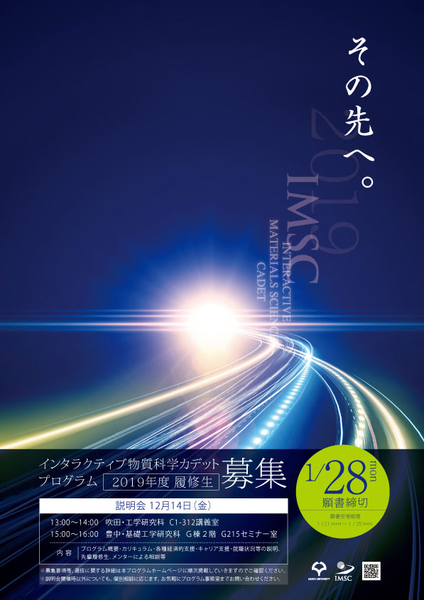
Program briefing session will be held
2018.12.14(Fri)
Program briefing session will be held for the student who is considering going to graduate school next spring.
【Suita campus】
date: Dec 14(Fri.) 13:00~14:00
Place: 312, C1 Building, Graduate School of Engineering
【Toyonaka campus】
date: Dec 14(Fri.) 15:00~16:00
Place: G215, Graduate School of Engineering Science
⇒Application Gidelines (Sorry, this entry is only available in Japanese)
Warning: Trying to access array offset on false in /home/autre/osaka-u.ac.jp/public_html/www.msc/wp-content/themes/imsc/category.php on line 234
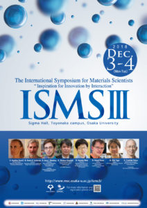
“The International Symposium for Materials Scientists III” will be held.
2018.12.3(Mon)
On December 3-4, Interactive Materials Science Cadet Program will host the International Symposium for Materials Scientists III (ISMS III) at Sigma Hall (Osaka University, Toyonaka Campus).
Warning: Trying to access array offset on false in /home/autre/osaka-u.ac.jp/public_html/www.msc/wp-content/themes/imsc/category.php on line 234
” Hong Kong – Osaka University 2nd Joint Symposium on Materials Research” will be held.
2018.12.3(Mon)
On December 3-4, Interactive Materials Science Cadet Program will host Hong Kong – Osaka University 2nd Joint Symposium on Materials Research, at Nambu Yoichiro Hall (Osaka University, Toyonaka Campus).

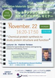
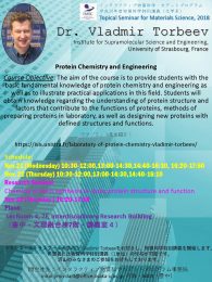
Topical Seminar by Dr.Vladimir Torbeev of University of Strasbourg
2018.11.21(Wed)
Topical Seminar for IMSC 2018 will be held.
Lecturer: Dr. Vladimir Torbeev
Institute for Supramolecular Science and Engineering, University of Strasbourg
Title: Introduction to soft matter and molecular ferroelectric science
Course objectives:
The aim of the course is to provide students with the basic fundamental knowledge of
protein chemistry and engineering as well as to illustrate practical applications in this field.
Students will obtain knowledge regarding the understanding of protein structure and factors
that contribute to the functions of proteins, methods of preparing proteins in laboratory,
as well as designing new proteins with defined structures and functions.
Schedule:
Nov.21 (Wednesday) 10:30-12:00,13:00-14:30,14:40-16:10, 16:20-17:50
Nov. 22 (Thursday) 10:30-12:00,13:00-14:30,14:40-16:10
Research Seminar:
"Chemical protein synthesis to study protein structure and function"
Nov.22 (Thursday ) 16:20-17:50
Place:
LecRoom 4, 7F, Interdisciplinary Research Building
Warning: Trying to access array offset on false in /home/autre/osaka-u.ac.jp/public_html/www.msc/wp-content/themes/imsc/category.php on line 234
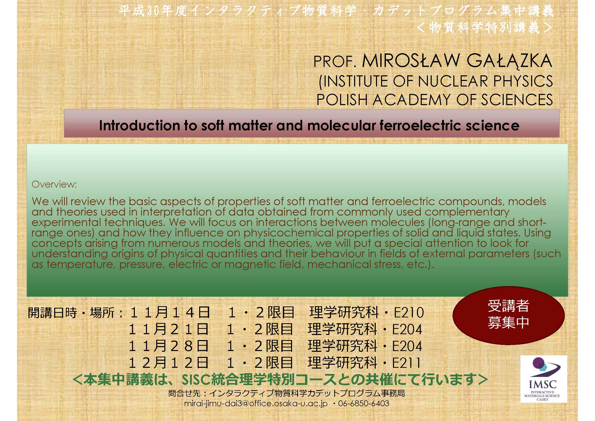
Topical Seminar by Mirosław Gałązka of Polish Academy of Sciences
2018.11.14(Wed)
Topical Seminar for IMSC 2018 will be held.
Lecturer: Mirosław Gałązka, Institute of Nuclear Physics, Polish Academy of Sciences
Title: Introduction to soft matter and molecular ferroelectric science
Schedule & Place:
Day 1: Nov. 14, 8:50-10:20, 10:30-12:00 (E210, Buildings of Graduate School of Science)
Day 2: Nov. 21, 8:50-10:20, 10:30-12:00 (E204, Buildings of Graduate School of Science)
Day 3: Nov. 28, 8:50-10:20, 10:30-12:00 (E204, Buildings of Graduate School of Science)
Day 4: Dec. 12, 8:50-10:20, 10:30-12:00 (E211, Buildings of Graduate School of Science)
Warning: Trying to access array offset on false in /home/autre/osaka-u.ac.jp/public_html/www.msc/wp-content/themes/imsc/category.php on line 234
Topical Seminar by Dr. H.Hirao of City University of Hong Kong
2018.8.21(Tue)
Topical Seminar for IMSC 2018 will be held.
Lecturer: Dr. Hajime HiraoDepartmentof Chemistry, City University of Hong Kong
Title: Introduction to Computational Chemistry
Course Objective:
Computational chemistry is nowadays an indispensable tool for investigating a variety of chemical phenomena at the atomic level. The availability of many elaborate software packages allows us to apply computational chemistry techniques to specific problems immediately without paying much attention to underlying theories. Although this black-box-like nature is in a sense a good aspect of computational chemistry, in this course, emphasis will be placed rather on discussing derivation processes and other details of a few fundamental concepts.
Schedule
Day 1: Aug. 21, 13:00-14:30, 14:40-16:10
Day 2: Aug. 22, 13:00-14:30, 14:40-16:10
Day 3: Aug. 23, 13:00-14:30, 14:40-16:10
Research seminar:
“Applications of Computational Chemistry to Chemical Reactions”
Aug.23,16:20-
Place
LecRoom 3, 7F, Interdisciplinary Research Building
Room F390, First Research Building of I.S.I.R*
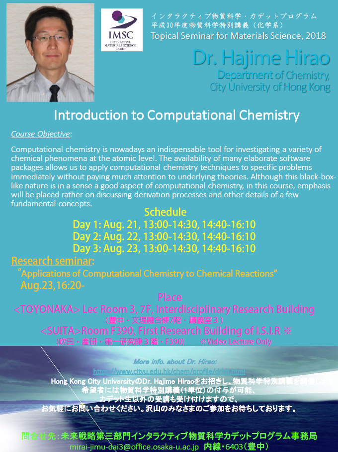
For more info., please contact IMSC office.
Warning: Trying to access array offset on false in /home/autre/osaka-u.ac.jp/public_html/www.msc/wp-content/themes/imsc/category.php on line 234
Syposium on “Diverse Facets of Chemistry Ⅱ”
2018.6.14(Thu)
Cadet Program will have guests from Strasbourg University, and have joint symposium.
Symposium title: Diverse Facets of ChemistryⅡ
Date: June 14-15, 2018
Place: Nambu Yoichiro Hall, Toyonaka Campus Osaka University
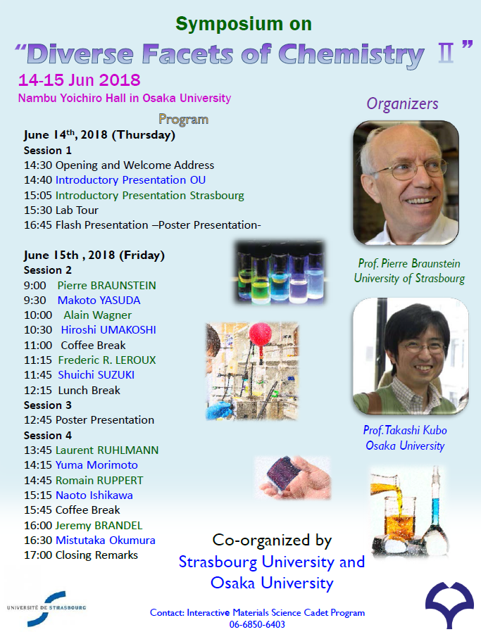
For inquiries: IMSC office 06-6850-6403
Warning: Trying to access array offset on false in /home/autre/osaka-u.ac.jp/public_html/www.msc/wp-content/themes/imsc/category.php on line 234
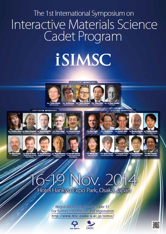
1st International Symposium on Interactive Material Science Cadet Program
2014.11.17(Mon)
General Information
- Date : Nov. 17-19, 2014
- Place : Hotel Hankyu Expo Park, Osaka, Japan
- Organizer : Professor Tsuyoshi Kimura, Graduate School of Engineering Science, Osaka University
- Abstract Submission : by the August 30, 2014[Student], by the September 22, 2014[Other]
- Registration : by the end of October, 2014
- Board size for each poster : A0 size (hight : 1189 mm × bredth 841 mm)
Warning: Trying to access array offset on false in /home/autre/osaka-u.ac.jp/public_html/www.msc/wp-content/themes/imsc/category.php on line 234
A poster of the 1st International Symposium on Interactive Materials Science Cadet Program
2014.11.16(Sun)
To Registration [The 1st International Symposium on Interactive Materials Science Cadet Program]
All students and staff are welcome to attend !
Warning: Trying to access array offset on false in /home/autre/osaka-u.ac.jp/public_html/www.msc/wp-content/themes/imsc/category.php on line 234
Topical Seminar for Materials Science by Prof. Tom Gregorkiewicz
2014.7.1(Tue)
Lecturer :Dr. Tom Gregorkiewicz (University of Amsterdam)
Date :
7/1 Tue 3rd・4th period
7/2 Wed 3rd・4th period
7/4 Fri 3rd・4th period
7/8 Tue 3rd・4th period
(date:7/9 Wed、11 Fri 3rd・4th period)
Place : R2 Build. of Engineering, 720 Seminar Room Ⅱ
Title :Photovoltaics for energy
Background :Tom Gregorkiewicz is full professor of Optoelectronic Materials at the Van der Waals-Zeeman Institute of the University of Amsterdam.
He has obtained his PhD (1980) at the Institute of Physics, Polish Academy of Sciences on the subject of defects in silicon. After a postdoc period, he is since 1989 staff member of the Science Faculty at the University of Amsterdam ? initially as assistant professor, and since 2003, as full professor.
In 2004 he received also the personal professorship from the President of the Republic of Poland. He is currently leading a research group at the Van der Waals-Zeeman Institute, working on optical properties of silicon nanostructures and is an academic teacher on both undergraduate and graduate levels.
To date he has published over 225 papers in refereed journals and has given more than 80 invited presentations at international meetings.
He organized several scientific conferences and symposia and is a member of multiple advisory and supervisory boards.
Warning: Trying to access array offset on false in /home/autre/osaka-u.ac.jp/public_html/www.msc/wp-content/themes/imsc/category.php on line 234
The 4th Solid-State Physics Seminar
2014.6.27(Fri)
Date : June 27, 2014 14:45-16:15
Place : A403 (4F of Bulid. A, Graduate School of Engineering Science)
Lecturer : Prof. Yoshinori TOKURA
(Director of Center for Emergent Matter Science, RIKEN)
Title :How to make magneto-electronic responses gigantic in condensed matters
Contact information : Tsuyoshi KIMURA
Tel : 06-6850-6455
E-mail : kimura@mp.es.osaka-u.ac.jp
Warning: Trying to access array offset on false in /home/autre/osaka-u.ac.jp/public_html/www.msc/wp-content/themes/imsc/category.php on line 234
The 3rd Solid-State Physics Seminar
2014.6.27(Fri)
Date : June 27, 2014 13:00-14:30
Place : A403 (4F of Bulid. A, Graduate School of Engineering Science)
Lecturer : Prof. Yoshihiko KANEMITSU
(Photonic Elements Science, International Research Center for Elements Science,
Institute for Chemical Research, Kyoto University)
Title : Multiple exciton and photonics in nanostructure semiconductor
Contact information : Masaaki ASHIDA
Tel : 06-6850-6426
E-mail : ashida@mp.es.osaka-u.ac.jp
Warning: Trying to access array offset on false in /home/autre/osaka-u.ac.jp/public_html/www.msc/wp-content/themes/imsc/category.php on line 234
Topical Seminar for Materials Science by Prof. Andreas Danopoulos
2014.6.24(Tue)
Lecturer:Prof. Andreas Danopoulos (University of Strasbourg, France)
Date:
6/24 Tue 2nd・3rd period
6/26 Wed 2nd・3rd period
7/2 Wed 2nd・3rd period
7/3 Thu 2nd period
7/3 Thu 3rd period(seminar, Place:D build. of Engineering Science 4F)
Place:Engineering Science JB07-09 Cadet Program Lecture Room
Thitle:Some current topics in coordination chemistry and their catalytic relevance
Background:He obtained his Ph. D. from the University of Athens, Greece. After collaborations with Geoffrey Wilkinson (Nobel laureate in Chemistry) at Imperial College London, and Malcolm Green at the University of Oxford, he created a team at the University of Southampton. Danopoulos was recipient of a Gutenberg Chair of Excellence (2010), which affiliated him with the Laboratoire de Chimie de Coordination (Institut de Chimie, UMR 7177 CNRS) and enabled him to inititate collaborations with other scientists from the University of Strasbourg, where he is currently a CNRS associated researcher.